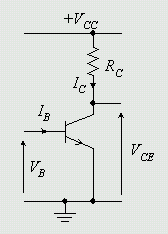
In these pages, we discuss three amplifier configurations, the amplifier class A, class B and class AB. Class of amplifier is distinguished by the location of the work load point of the transistor. Load point is located in the load line as shown in Figure 2, assuming the transistor circuit is the common emitter configuration (as in Figure 1).
Transistor in the circuit in Figure 1, will have a working point between points A and B, along the load line. Point A is the working area when the transistor is experiencing saturation, while point B is when the transistor cut-off.
Class A Amplifier
The point of the load transistors in class A amplifier is placed between points A and B, usually to produce a good performance then the point load is placed right in the middle of the load line. This has meant that the output signal will have a form of signal symmetry between positive and negative cycles. In order to obtain the exact middle point of the load, then VCE is designed to be equal to VCC / 2. To produce this, the IB is designed to produce the ICRC together with VCC / 2. Class A amplifier can be realized with the circuit as Figure 3 below.
Class A amplifier is designed to strengthen the small signals. While the shortcomings of the amplifier of this type is when there is no input signal, the transistor will still consume electricity.
Class B Amplifier
The amplifier is realized by assembling a pair of complementary transistors as shown in Figure 4. Unlike the class A amplifier, the load point of the class B amplifier transistor pad placed point B (the cut-off). With these conditions, then when there is no input signal, the transistor does not consume electricity. The amplifier of this type is also known as push-pull amplifier as the work of the transistor pair is alternately. This amplifier is applied as the final amplifier, or a large signal amplifier.
When Vin is in the positive phase only NPN transistor is ON, while when the signal Vin is in the negative phase only the PNP transistor is ON. However, because the bias voltage of the transistor from the signal Vin, the signal will be clipped by the VBE voltage, so that the output signal will experience a disability (distortion).
Class AB amplifiers
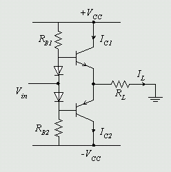
To overcome the distortion of the amplifier permaslahan class B, then made a class AB amplifier. This amplifier has a load point is located slightly above the point B (Figure 2), the transistor in the tegnagn dibias threshold condition of VBE. In this condition, then in a state with no signal Vin, the transistor does not consume electricity. Meanwhile, when Vin comes up then this signal is not interrupted by the signal output voltage VBE that is not distorted. Example of a class AB amplifier is as
Class A Amplifier
The point of the load transistors in class A amplifier is placed between points A and B, usually to produce a good performance then the point load is placed right in the middle of the load line. This has meant that the output signal will have a form of signal symmetry between positive and negative cycles. In order to obtain the exact middle point of the load, then VCE is designed to be equal to VCC / 2. To produce this, the IB is designed to produce the ICRC together with VCC / 2. Class A amplifier can be realized with the circuit as Figure 3 below.
 |
| Figure 3. Amplifier class A. |
Class A amplifier is designed to strengthen the small signals. While the shortcomings of the amplifier of this type is when there is no input signal, the transistor will still consume electricity.
Class B Amplifier
The amplifier is realized by assembling a pair of complementary transistors as shown in Figure 4. Unlike the class A amplifier, the load point of the class B amplifier transistor pad placed point B (the cut-off). With these conditions, then when there is no input signal, the transistor does not consume electricity. The amplifier of this type is also known as push-pull amplifier as the work of the transistor pair is alternately. This amplifier is applied as the final amplifier, or a large signal amplifier.
 |
Figure 4. Class B amplifier (push-pull). |
Class AB amplifiers
To overcome the distortion of the amplifier permaslahan class B, then made a class AB amplifier. This amplifier has a load point is located slightly above the point B (Figure 2), the transistor in the tegnagn dibias threshold condition of VBE. In this condition, then in a state with no signal Vin, the transistor does not consume electricity. Meanwhile, when Vin comes up then this signal is not interrupted by the signal output voltage VBE that is not distorted. Example of a class AB amplifier is as
 |
| Figure 5. Class AB amplifiers |

0 Response to "Amplifier Classes Circuit"
Post a Comment